News
Growing 2D semiconductors the easy way
Oct 6, 2014
By Belle Dumé
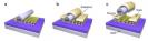
Researchers at the University of California at Los Angeles in the US and Hunan University in Changsha, China, have come up with a new way to grow 2D-layered semiconductor heterostructures whose composition can be controlled by modulating the constituent vapour-phase reactants during growth. The structures produced are single crystals and might be used to make a host of electronics devices, ranging from complementary logic circuits, photovoltaics and photodetectors, to light-emitting diodes and laser diodes...
[via nanotechweb.org]
UCLA, Department of Chemistry and Biochemistry
607 Charles E. Young Drive East, Box 951569
Los Angeles, CA 90095-1569
E-mail: xduan@chem.ucla.edu
607 Charles E. Young Drive East, Box 951569
Los Angeles, CA 90095-1569
E-mail: xduan@chem.ucla.edu


